- 1 Questions
- 2 A load of articles/blogs/pages to read
- 2.1 Wikipedia articles
- 2.2 More posts
- 2.3 Notes
- 2.4 My own RAM
- 2.5 Continued notes
- 2.6 Address mapping notation
- 2.7 Intel spec
- 2.8 Rank interleaving
- 2.9 Nontemporal reads/writes
- 3 reMap: using Performance counters
- 4 Sudoku
- 5 Sudoku, now with only 1 DIMM
- 6 Final results
- 7
decode-dimms- 7.1 Bank groups
- 7.2 Refresh
- 7.3 Random access throughput
- 8 CPU benchmarks
- 9
tinymembench - 10 Remaining questions
These are chronological (and thus, only lightly organized) notes on my attempt to understand how DDR4 and DDR5 RAM memory work.
See the final results for the conclusion on how virtual addresses map to physical addresses.
1 Questions Link to heading
Specific questions to be answered:
- How is data distributed among the chips?
- How does dual channel DDR work?
- And does the CPU become a bottleneck here?
- How does RAM work?
- Are there internal cache sizes?
- What is burst?
- Can we disable it?
- Can we read only a single word?
- And prefetching? (8n, 16n)
- Why? (reduce downtime / communication overhead)
- Stored how?
- Why does DDR5 have 2x32 lanes instead of DDR4’s 64bit lanes?
- How large are rows and columns?
- What about LPDDR (= lower power DDR)
- What’s a transfer anyway
- banks? bank groups?
- transferring to different bank groups is faster?
- DDR5: 2/4/8 bank groups
- How does virtual memory map to physical memory?
2 A load of articles/blogs/pages to read Link to heading
2.1 Wikipedia articles Link to heading
Wikipedia articles:
- DDR: https://en.wikipedia.org/wiki/DDR_SDRAM
- DDR4: https://en.wikipedia.org/wiki/DDR4_SDRAM
- DDR5: https://en.wikipedia.org/wiki/DDR5_SDRAM
- https://en.wikipedia.org/wiki/Synchronous_dynamic_random-access_memory#PREFETCH
- https://en.wikipedia.org/wiki/Interleaved_memory
- https://en.wikipedia.org/wiki/Memory_refresh
2.2 More posts Link to heading
- https://www.synopsys.com/blogs/chip-design/ddr-generations-memory-density-speed.html
- https://www.synopsys.com/articles/ddr4-bank-groups.html
- (Mahling, Weisgut, and Rabl 2025)
- https://api.drum.lib.umd.edu/server/api/core/bitstreams/5ec3f878-7a0d-4df8-a98f-1600b5c35e2b/content
- https://www.synopsys.com/blogs/chip-design/ddr5-technology-advancements-performance.html
- https://superuser.com/questions/1132788/what-is-a-ram-bank-how-is-it-defined
- book: DRAM Circuit Design: Fundamental and High-Speed Topics (IEEE Press Series on Microelectronic Systems)
- https://www.igorslab.de/en/ddr5-deep-dive-kingston-in-interview-about-new-memory-standard-and-examples-from-the-practice/2/
- long post explaining all timings: https://www.reddit.com/r/overclocking/comments/ahs5a2/demystifying_memory_overclocking_on_ryzen_oc/
- https://www.systemverilog.io/design/understanding-ddr4-timing-parameters/
- https://blog.cloudflare.com/ddr4-memory-organization-and-how-it-affects-memory-bandwidth/#:~:text=Multi%2Drank%20memory%20modules%20use,rank%20can%20start%20its%20transmission.
- https://medium.com/@mitali.soni04/decoding-dram-timings-part-i-4f97a5b90e82
- https://medium.com/@mitali.soni04/decoding-dram-timings-part-ii-9541e0f72aca
- https://www.forrestthewoods.com/blog/memory-bandwidth-napkin-math/
- https://www.youtube.com/watch?v=7J7X7aZvMXQ
- https://ieeexplore.ieee.org/document/6932587
- nice intro
2.3 Notes Link to heading
https://en.wikipedia.org/wiki/Synchronous_dynamic_random-access_memory#PREFETCH:
[DDR3] Row accesses might take 50 ns, depending on the speed of the DRAM, whereas column accesses off an open row are less than 10 ns.
DDR4 did not double the internal prefetch width again, but uses the same 8n prefetch as DDR3.[29] Thus, it will be necessary to interleave reads from several banks to keep the data bus busy.
https://api.drum.lib.umd.edu/server/api/core/bitstreams/5ec3f878-7a0d-4df8-a98f-1600b5c35e2b/content
- dual channel has 2 chips doing the exact same work, interleaving things at
the level of words: 64 bits to one and 64 bits to the other.
- Does this mean an effective RAM cache size of 1024 bits, given burst mode???
https://www.synopsys.com/articles/ddr4-bank-groups.html
- prefetch matches cacheline size
- DDR4: bank groups, so multiple reads can happen ‘in parallel’
- a prefetch happens within a bank group, but takes time
- 16n prefetch would be larger than a cacheline, not useful
- instead: 2 (or more) bank ground that work independently in parallel
- alternating groups is faster than consecutive reads in a group
- 4 cycles across groups; more within
- 1600MHz gives up to 3200Mb/s when alternating, or 2133Mb/s within the same group
- alternating between banks: can fully saturate the bandwidth with 4 internal cycles (8 transfers) between bursts
- on the same group, only as low as ~half the throughput
Dual-Channel Symmetric mode, also known as interleaved mode, provides maximum performance on real world applications. Addresses are ping-ponged between the channels after each cache line (64-byte boundary).
- out of all pending requests, efficient ones to be answered are chosen
https://en.wikipedia.org/wiki/Interleaved_memory
- row buffer typically has same size as OS memory page
https://ieeexplore.ieee.org/document/898056 (Zhang, Zhu, and Zhang 2000)
channel interleaveandrank interleavecan be changed in bios?
https://ee.usc.edu/~redekopp/ee457/slides/EE457Unit7b_Interleaving.pdf bank: byte-size memory
- nice figure
https://www.systemverilog.io/design/ddr4-basics/
- good figures
- each bank has multiple (4 or 8) memory arrays
- 512/1024/2048 page size = bits/row
- 1024 columns always
- variable number of rows
- width cascading: 128bit words by having half from each chip
https://www.systemverilog.io/design/lpddr5-tutorial-physical-structure/
synchronous vs async ram:
- sync: common clock frequency
2.4 My own RAM Link to heading
laptop model:
- HMAA4GS6AJR8N-XN
- https://www.compuram.biz/memory_module/sk-hynix/hmaa4gs6ajr8n-xn.htm
- 3200 MT/s
- 1600 MHz
- 32GB (2Rx8): 2 ranks, 8 bit data width / 8 banks
- 260pin
- 2 ranks
- number of dram: 16
- 2Gx8: 2GB per chip, within each rank?
- construction type: FBGA(78ball)
- unbuffered: more reliability by buffering data before sending it over
- organization: 4Gx64
- number of DRAM: 16
- DRAM organization: 2Gx8
2.5 Continued notes Link to heading
jedec standard: https://e2e.ti.com/cfs-file/__key/communityserver-discussions-components-files/196/JESD79_2D00_4.pdf
page 15: 2Gb x8 addressing:
- 4 bank groups (2bits)
- 4 banks inside a group (2bits)
- 17bit row ID => 128ki rows
- 10bit col ID => 1024 cols
- 1KB page size (#cols * 8 banks)
=> total page size for 8 chips: 8KB.
Possible experiment:
- read
a[i], where i iterates over the integers with only a fixed subset of bits set, like a mask of111101001110000. Trying all patterns, we can try to hit consecutive rows on the same bank. - multithreaded setting; always have a certain bit of the index at 0, the rest 1
- try to always hit the same bank
- try to always hit the same rank
Side note:
- L1 prefetch needs fill buffers, but the L2 hardware prefetcher does not!
gemini: cache lines are alternated between dimms/channels.
https://arxiv.org/html/2512.18300v1 (Jattke et al. 2024)
For example, modern memory mappings, such as AMD-Zen [11], split a 4KB page such that it gets distributed across 32 banks (with only two lines of a page co-resident in the same bank). Such mappings exploit the available bank-level parallelism for reads, even at the expense of the row-buffer hit-rate.
- interesting indeed: reading from different banks is faster than consecutive reads from a single row then
- more generally, I guess cachelines are round-robin between banks then
https://os.itec.kit.edu/3617_3389.php (Hillenbrand 2017)
https://docs.amd.com/r/en-US/pg313-network-on-chip/DDR4-Component-Choice
For a 64-bit DDR4 interface, this means the controller can support a single x64 channel, or dual x32 channels.
ie, there are cases where the two dimms do exactly the same work but on half the bits. Then additional bank (groups) are available for parallellism
with two memory controllers (same as channels or not?):
- memory can be interleaved at eg 1KB block size, or
- each controller is half the address space
https://news.ycombinator.com/item?id=30178764
https://ashvardanian.com/posts/ddr4-bandwidth/
https://adaptivesupport.amd.com/s/article/41169?language=en_US
https://docs.amd.com/r/en-US/ug585-zynq-7000-SoC-TRM/DDR-Efficiency
https://news.ycombinator.com/item?id=16172686
https://stackoverflow.com/questions/43343231/enhanced-rep-movsb-for-memcpy/43574756#43574756
https://www.reddit.com/r/cpp/comments/9ccb88/optimizing_cache_usage_with_nontemporal_accesses/
2.6 Address mapping notation Link to heading
This pages is really nice:
Example: 16R-2B-2BG-10C:
- ignore low 3 bits, because we get 64b = 8B = 2^3 B back.
- 10 bits for column. Ie a linear piece of memory fills a row.
- Each column is 64b = 8B across all banks, 1024 columns per row = 8KiB
- 2 bits for the bank group, ie spread 4 rows over 4 distinct bank groups
- 2 bits for bank, ie then take a row in each bank of each group
- 15 bits for row, ie then use the other rows in each bank
Reading consecutively from the same row (in the same bank) is slow though. So
instead, we can alternate bank group after every 64B cache line (aka bank group optimization):
16R-2B-1BG-7C-1BG-3C: this moves 1 BG bit to the end, so we interleave reads
to two bank groups to be able to fully saturate the bandwidth. This has 95%
efficiency, compared to 54% of the simple row-bank-column approach.
If addressing is random and transaction size is equal to the DRAM basic access unit, then no address mapping has an advantage. The DRAM controller will reorder transactions to hide page access overhead as much as possible. Expected efficiency is around 40%.
2.7 Intel spec Link to heading
Addresses are ping-ponged between the channels after each cache line (64-byte boundary).
5.1.5:
- just-in-time: most efficient request scheduled first, e.g., one that hits a different bank than the last instruction.
- command overlap: send stuff to other banks while one is doing slow activate/pre-charge/read/write
- out-of-order: batch requests to the same open page
2.8 Rank interleaving Link to heading
Multi-rank memory modules use a process called rank interleaving, where the ranks that are not accessed go through their refresh cycles in parallel
On the other hand, there is some I/O latency penalty with multi-rank memory modules, since memory controllers need additional clock cycles to move from one rank to another.
one row can remain active per bank
2.9 Nontemporal reads/writes Link to heading
https://vgatherps.github.io/2018-09-02-nontemporal/
https://www.reddit.com/r/cpp/comments/9ccb88/optimizing_cache_usage_with_nontemporal_accesses/
because they are only beneficial if you can prove that the address being stored to is not in cache, and would not be present in cache at next use even if a normal store were used.
they break some of the usual ordering guarantees.
the performance is catastrophically bad (significantly worse than normal stores) when the address is present in cache.
https://sites.utexas.edu/jdm4372/2018/01/01/notes-on-non-temporal-aka-streaming-stores/
https://blogs.fau.de/hager/archives/2103
3 reMap: using Performance counters Link to heading
https://github.com/helchr/reMap
Helm, Akiyama, and Taura (2020) uses performance counters to read directly how many times each rank/bank group/bank is accessed.
It uses stuff from /sys/bus/event_source/devices/uncore_imc/
type is 14.
here https://stackoverflow.com/questions/64923795/using-linux-perf-tool-to-measure-the-amount-of-times-the-cpu-has-to-acccess-the I read that only Xeon/servers have these cas counters.
Performance counter monitor: https://github.com/intel/pcm
pcm-memorywith per-bank stats only works on Xeon unfortunately
4 Sudoku Link to heading
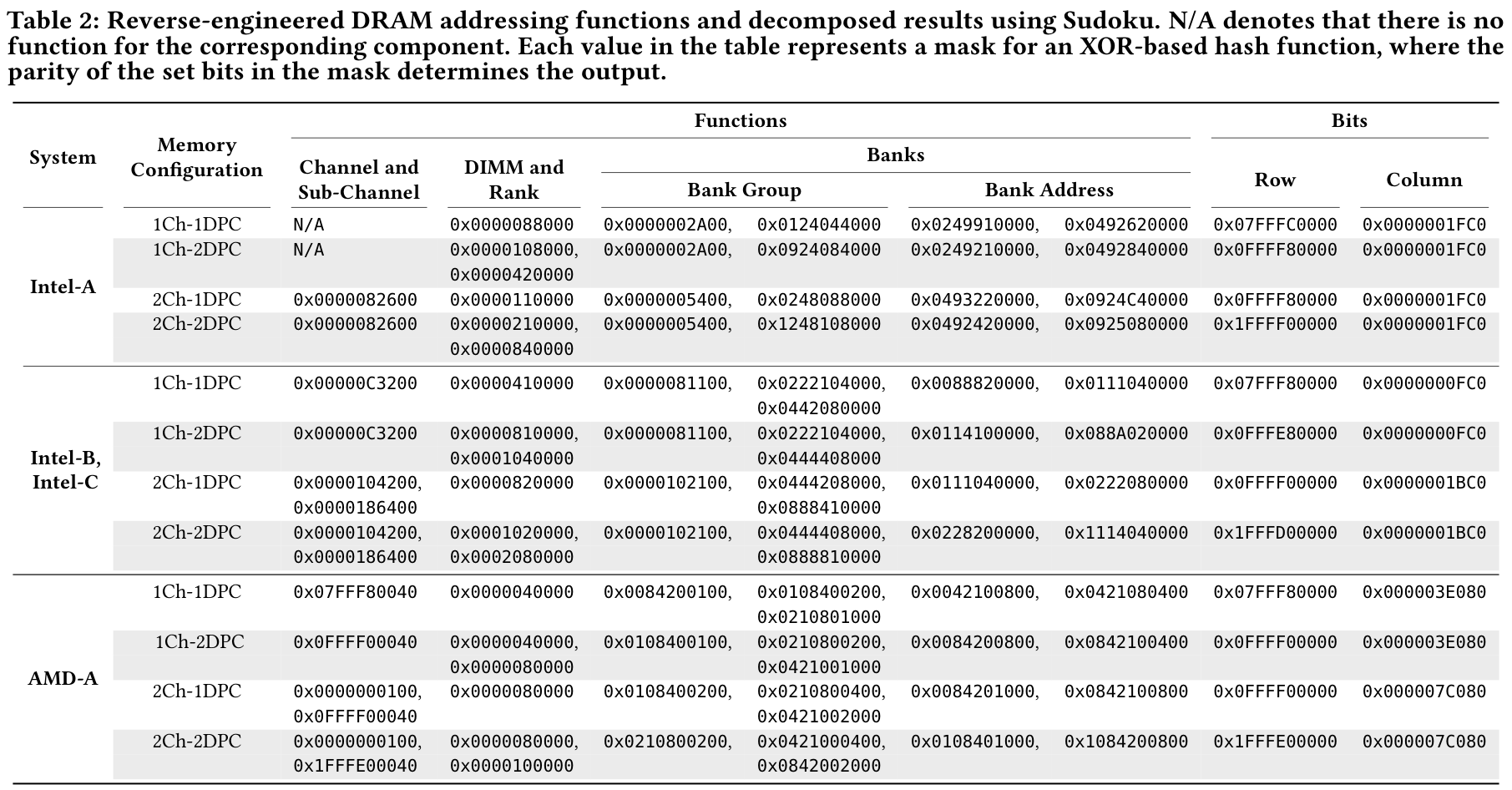
Really cool paper and software: “Sudoku: Decomposing Dram Address Mapping into Component Functions” (Wi et al. 2025). https://github.com/scale-snu/Sudoku
hugepages setup:
| |
speed:
| |
memory config:
| |
I also incremented max_bits_ by 2 in the Sudoku constructor. Not exactly sure why it’s needed.
We also pin the cpu frequency to 3.0GHz (slightly above the native 2.6GHz):
| |
4.1 Step 1: DRAM addressing functions Link to heading
ie things that map to the same bank
command:
| |
functions:
| |
4.2 Step 2: row/column bits Link to heading
| |
result with masking: column bits: 0xdc0 row_bits,0xffff80000 column_bits,0xdc0
Note that some column bits are still missing, as 0xdc0 = 1101 1100b only has 5
instead of 7 bits set. (We are looking for 7 bits, because each column has \(2^{10}\)
64-bit words and thus \(2^7\) cache lines.)
4.3 Step 3: validation Link to heading
| |
| |
So real column should be 0x1FC0, exactly the same as in Table 2 in the paper for another intel DDR4 machine. (That only has 7 bits, because the last 3 column bits indicate 8 64bit words that always share a cacheline [I think].)
We get:
| |
4.4 Step 4: which function is what? Link to heading
Lets first have a manual look at these functions:
| |
They use 36 bits, corresponding to \(2^{36} = 64\) GiB of data.
Also note that the low 6 bits are 0, because we have \(2^6=64\) byte cache lines.
Some [wrong] guesses. We already know the row and column bits, but the rest is speculation for now. Looking at the Sudoku paper, we need 4 functions for banks and bank groups, so I would speculate that’s the four very similar ones. Then we need 2 to select the DIMM and rank within a channel (because each channel could have 2 rank-2 memory sticks), so I’d guess the two similar patterns that remain. Specifically, that would mean the highest bit determines the DIMM, of which I only have 1 in each channel, and thus be unused.
That leaves one ‘weird’/‘chaotic’ pattern for the channel, which also seems to match the Sudoku table (Wi et al. 2025):
4.5 Refreshes Link to heading
Now lets have a look at the output of decompose_functions, which does
additional experiments to distinguish DIMMs/ranks/bank groups/bank.
| |
Specifically, it chooses two addresses that only differ by a given function and
then alternatingly reads them. DRAM needs regular ‘refreshing’, every 64ms or so, which for my
hardware takes tRFC1 = 350ns. This can be done one either one bank at a time,
or for all banks simultaneously.
If we now choose 2 addresses and read them alternatingly, we will see one of two patterns. If they are in the same refresh group, we will see a single refresh delay every refresh cycle. If they are in different refresh groups, we will see two refresh patterns interleaved.
You might need to play a bit with the REGULAR_REFRESH_INTERVAL_THRESHOLD parameter.
We get:
| |
These numbers mean the following: for 5 of the 6 functions, we consistently
observe a tREFI delay, which is the refresh interval. (I still have not found
a way to extract the actual value of number from my hardware.)
The 0x10000 function on the other hand consistently shows a smaller interval
between refreshes, meaning that this switches data to a different refresh group.
Thus, I speculate that 0x110000 determines the DIMM, and all banks on each
DIMM (across both ranks) refresh at the same time.
See also Auto-refresh (AR) on wikipedia.
4.6 Consecutive Accesses Link to heading
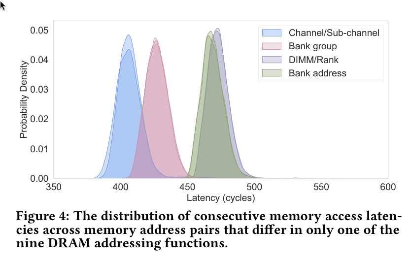
Now we look at the time between consecutive accesses, tRDRD (time ReaD ReaD)
and specifically tCCD_S and tCCD_L, the time between consecutive reads in
different (S, short) and the same (L, long) bank groups, assuming row-buffer hits.
For this, the tool schedules 4 consecutive reads from each of two rows and lets
the memory controller execute them as fast as possible.
We get this:
| |
Latency here represents the number of clock cycles to read a total of 8 values.
Based on the paper, alternating between channels should be fastest, followed by bank groups. Alternating between banks and Rank is slower.
My guesses are based on correlating these results with the plot from the Sudoku paper:
| refresh group | read-read | what | |
|---|---|---|---|
000000000000000000000001111111000000 | col | ||
000000000000000000000100000010000000 | same | 347 | bank group / channel |
000000000000000001001011001100000000 | same | 346 | bank group / channel |
000000000000000010001000000000000000 | same | 345 | bank group / channel |
000000000000000100010000000000000000 | different | 400 | rank/channel? |
000000000000001000100000000000000000 | same | 396 | bank |
000000000000010001000000000000000000 | same | 397 | bank |
111111111111111110000000000000000000 | row |
Correlating with row Intel-A 2-channels 1-dimm-per-channel from the table above:
| what | |
|---|---|
000000000000000000000001111111000000 | col |
000000000000000010000010011000000000 | channel |
000000000000000000000101010000000000 | group |
001001001000000010001000000000000000 | group |
000000000000000100010000000000000000 | rank |
010010010011001000100000000000000000 | bank |
100100100100110001000000000000000000 | bank |
111111111111111110000000000000000000 | row |
Things look quite similar and so my guess is that the order of things is indeed the same:
| refresh group | read-read | what | |
|---|---|---|---|
000000000000000000000001111111000000 | col | ||
000000000000000000000100000010000000 | same?? | 347 | channel |
000000000000000001001011001100000000 | same | 346 | group |
000000000000000010001000000000000000 | same | 345 | group |
000000000000000100010000000000000000 | different | 400 | rank |
000000000000001000100000000000000000 | same | 396 | bank |
000000000000010001000000000000000000 | same | 397 | bank |
111111111111111110000000000000000000 | row |
5 Sudoku, now with only 1 DIMM Link to heading
5.1 setup Link to heading
- Allocate 20 1GB hugepages
- Add an entry to the table with 32 GB.
1{DDRType::DDR4, 32ULL * GB, 8, 2, 2, 17, 10, 8 * 1024, 8},
5.2 1. reverse functions Link to heading
- run the same command as before, but now for 1 DIMM and 20 pages:
1sudo ./reverse_functions -o out -p 17 -t ddr4 -n 1 -s 32 -r 2 -w 8 -d -v -l
Changes to make it work: Change timing to
| |
and use the median instead of average time.
This outputs:
| |
5.3 2. identify bits Link to heading
| |
with original max_bits or +1:
| |
The only issue here is that this has only 16 row bits. Likely it doesn’t detect
the last one because I only have slightly over half of the memory used. Either
way we can assume that the real row bits should be 0x7fffc0000
5.4 3. validate mapping Link to heading
| |
5.5 4. decompose functions Link to heading
| |
The situation is more clear now: the interleaved refresh intervals are across the two ranks. And then the 2 fast RDRD latencies are across groups and the two slow ones across banks.
| |
New table:
| refresh group | read-read | what | |
|---|---|---|---|
00000000000000000000001111111000000 | col | ||
00000000000000000000010000001000000 | same | 346 | group |
00000000000000001000100000000000000 | same | 342 | group |
00000000000000010001000000000000000 | different | 403 | rank |
00000000000000100010000000000000000 | same | 390 | bank |
00000000000001000100000000000000000 | same | 393 | bank |
11111111111111111000000000000000000 | row |
6 Final results Link to heading
| 1 DIMM (32 GB) | what | 2 DIMM (64 GB) | what |
|---|---|---|---|
00000000000000000000001111111 | col | 000000000000000000000001111111 | col |
00000000000000000000010000001 | group | 000000000000000000000100000010 | channel |
| - | 000000000000000001001011001100 | group | |
00000000000000001000100000000 | group | 000000000000000010001000000000 | group |
00000000000000010001000000000 | rank | 000000000000000100010000000000 | rank |
00000000000000100010000000000 | bank | 000000000000001000100000000000 | bank |
00000000000001000100000000000 | bank | 000000000000010001000000000000 | bank |
11111111111111111000000000000 | row | 111111111111111110000000000000 | row |
Summary on how to interpret this:
colindicates that the low 7 bits are used to indicate the column to read from.rowindicates that the high 16 or 17 bits determine the row to read from.- All other masks indicate that the xor of the indicated address-bits is taken, and the parity determines the channel/rank/group/bank. Each rank has 4 groups containing 4 banks each, so these get 2 bits assigned to them.
In general these look very similar. Differences:
- With 2 DIMMs, pairs of cachelines go next to each other in the same row. With 1, they are scattered across groups.
- With 2 DIMMs, the lowest level scattering is changed to channels. The first group-scatter gets a somewhat random mask.
7 decode-dimms
Link to heading
Here I’m logging the output of running some analysis tools.
decode-dimms, part of i2c-tools, on arch is a nice tool to read
information from memory module EEPROM.
But note that this is static information, and not the current mode.
For me it prints eg:
| |
This confirms some information we already knew by now:
- 2 ranks per DIMM
- 10 column bits, 17 row bits, and 16 banks.
The question is how relevant the timing parameters are if these are not necessarily the current values.
7.1 Bank groups Link to heading
reading from different bank groups takes the minimum of 4 cycles (in which 8 words are transmitted)
7.2 Refresh Link to heading
64ms between refreshes, split in 8192 groups, so 64ms/8192=7.8us on average between refresh calls
Each call is around 350ns=4.5% long, blocking the entire rank.
7.3 Random access throughput Link to heading
Limitations:
- opening a single row in a bank
- tRCD = 13.750 ns to move row into amplifiers
- tRAS = 32.000 ns to move it back
- between reads in a group: 4.9ns
- between reads across groups: 2.5ns
- but either way: at most 4 reads on the rank every 21ns => 5.25 ns/read limit per rank (or DIMM?)
8 CPU benchmarks Link to heading
Lastly, some benchmarks, run with both 1 and 2 DIMMs.
8.1 cpu-benchmarks Link to heading
See /posts/cpu-benchmarks/ and github:RagnarGrootKoerkamp/cpu-benchmarks.
8.1.1 random access throughput 1 DIMM Link to heading
| |
| |
8.1.2 random access throughput 2 DIMM Link to heading
| |
| |
8.2 memory-read-experiment Link to heading
See github:feldroop/memory-read-experiment
8.2.1 strided reading 1 DIMM Link to heading
| |
8.2.2 strided reading 2 DIMM Link to heading
| |
9 tinymembench
Link to heading
https://github.com/ssvb/tinymembench
Nontemporal writes get to 44 GB/s, which is not too far of the max of
2*25.6=51.2 GB/s. This corresponds to 1.45 ns/cacheline, which is a bit faster
than the best of 1.72 ns/cacheline we observed above for streaming reads.
| |
10 Remaining questions Link to heading
- Why do we not so interleaved refresh intervals between reads from different
DIMMs?
- Speculative answer: they auto-synchronize. As soon as 1 starts a refresh, the other becomes idle and will also refresh.
- Why is alternating reads between channels not faster than alternating between
groups?
- I guess because both are maximally fast?
- Why is alternating reads between ranks quite a bit slower?
- No ideas here; the rank-to-rank switching time should be only a single cycle or so.
- How do things change on big servers (EPYC) with multiple memory controllers?
- Does sending read instructions consume a cycle? Can reading and controlling happen in parallel?